
Direct light-to-token conversion with integrated 2D photosensitive memory
Abstract
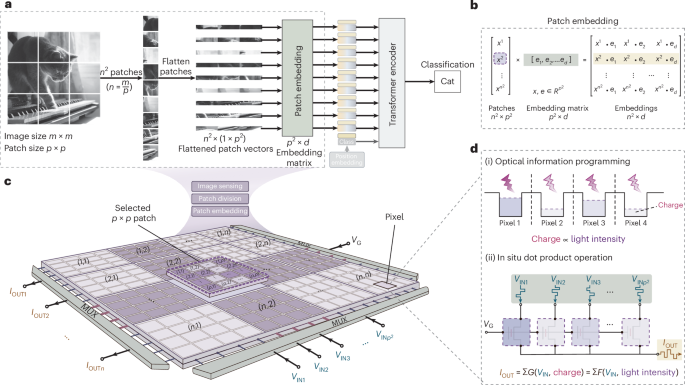
Vision transformers (ViTs) process images as sequences of embedded tokens, yet in existing architectures, tokenization is performed entirely in the digital domain, downstream of image capture. This separation increases energy cost and prevents token formation from occurring where visual information is physically generated. Here we introduce a physical tokenizer that performs analogue light-to-token conversion directly at the sensor level for ViTs. The prototype integrates a 32 × 32 photosensitive memory array of monolayer MoS2 floating-gate phototransistors with peripheral addressing circuitry, enabling optical images to be stored as non-volatile states and selectively combined into patch embeddings in situ, thereby eliminating separate sensing, patch division and patch embedding stages. When deployed in a standard ViT pipeline, the physical tokenizer achieves software-comparable accuracy on CIFAR-10 while reducing energy consumption by 14.3-fold relative to a digital tokenizer. These results establish physical tokenization as an energy-efficient and scalable hardware foundation for edge-intelligent, data-intensive vision systems.
This is a preview of subscription content, access via your institution
Access options
Access through your institution
Subscribe to this journal
Receive 12 digital issues and online access to articles
111,21 € per year
only 9,27 € per issue
Buy this article
- Purchase on SpringerLink
- Instant access to the full article PDF.
- Two-dimensional materials
- Received: 09 December 2025
- Accepted: 14 July 2026
- Published: 19 August 2026
- Version of record: 19 August 2026
- DOI: https://doi.org/10.1038/s44460-026-00122-3
39,95 €
Prices may be subject to local taxes which are calculated during checkout
Fig. 1: Architecture of a physical tokenizer.
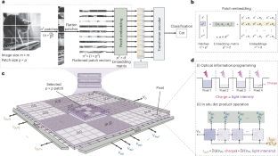
Fig. 2: Characterization of the photosensitive memory array.
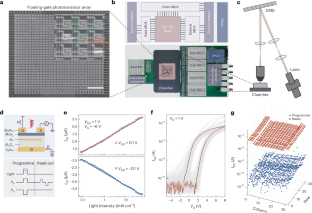
Fig. 3: Hardware implementation of physical tokenization.
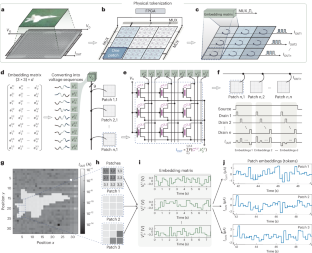
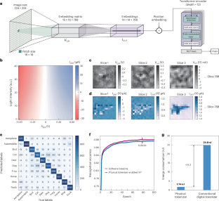
Fig. 4: Physical tokenizer-enabled ViT for image classification.
Bioinspired phototransistor with tunable sensitivity for low-contrast target detection
Article Open access 01 January 2026
In-sensor analog optoelectronic processing of concurrent event and memory signals for dynamic vision sensing
Article Open access 26 December 2025
Parallelizing analog in-sensor visual processing with arrays of gate-tunable silicon photodetectors
Article Open access 21 May 2025
Subjects
Data availability
The data supporting the findings of this study are available from the corresponding authors upon reasonable request. Source data are provided with this paper.
Code availability
The code supporting the findings of this study is available from the corresponding authors upon reasonable request.
References
1. Dosovitskiy, A. et al. An image is worth 16 × 16 words: transformers for image recognition at scale. In Proc. International Conference on Learning Representations (ICLR, 2021). 2. Liu, Z. et al. Swin transformer: hierarchical vision transformer using shifted windows. In Proc. IEEE/CVF International Conference on Computer Vision 10012–10022 (IEEE, 2021). 3. Han, K. et al. A survey on vision transformer. IEEE Trans. Pattern Anal. Mach. Intell. 45, 87–110 (2023). Article PubMed Google Scholar 4. Wu, B. et al. Visual transformers: token-based image representation and processing for computer vision. Preprint at <https://arxiv.org/abs/2006.03677> (2020). 5. Khan, S. et al. Transformers in vision: a survey. ACM Comput. Surv. 54, 200 (2022). Article Google Scholar 6. Sun, M. et al. VAQF: fully automatic software–hardware co-design framework for low-bit vision transformer. Preprint at <https://arxiv.org/abs/2201.06618> (2022). 7. Wang, T. et al. ViA: a novel vision-transformer accelerator based on FPGA. IEEE Trans. Comput.-Aided Des. Integr. Circuits Syst. 41, 4088–4099 (2022). Article Google Scholar 8. Zidan, M. A., Strachan, J. P. & Lu, W. D. The future of electronics based on memristive systems. Nat. Electron. 1, 22–29 (2018). Article Google Scholar 9. Zhou, F. & Chai, Y. Near-sensor and in-sensor computing. Nat. Electron. 3, 664–671 (2020). Article Google Scholar 10. Shi, W., Cao, J., Zhang, Q., Li, Y. & Xu, L. Edge computing: vision and challenges. IEEE Internet Things J. 3, 637–646 (2016). Article Google Scholar 11. Ren, Q. et al. Optoelectronic devices for in-sensor computing. Adv. Mater. 37, 2407476 (2025). Article CAS PubMed Google Scholar 12. Wang, S. et al. Nonvolatile van der Waals heterostructure phototransistor for encrypted optoelectronic logic circuit. ACS Nano 16, 4528–4535 (2022). Article CAS PubMed Google Scholar 13. Wang, J. et al. Technology and integration roadmap for optoelectronic memristor. Adv. Mater. 36, e2307393 (2024). Article PubMed Google Scholar 14. Zhou, F. et al. Optoelectronic resistive random access memory for neuromorphic vision sensors. Nat. Nanotechnol. 14, 776–782 (2019). Article CAS PubMed Google Scholar 15. Zhou, G. et al. Full hardware implementation of neuromorphic visual system based on multimodal optoelectronic resistive memory arrays for versatile image processing. Nat. Commun. 14, 8489 (2023). Article CAS PubMed PubMed Central Google Scholar 16. Jang, H. et al. An atomically thin optoelectronic machine vision processor. Adv. Mater. 32, e2002431 (2020). Article PubMed Google Scholar 17. Huang, H. et al. Fully integrated multi-mode optoelectronic memristor array for diversified in-sensor computing. Nat. Nanotechnol. 20, 93–103 (2025). Article CAS PubMed Google Scholar 18. Zhang, Z. et al. All-in-one two-dimensional retinomorphic hardware device for motion detection and recognition. Nat. Nanotechnol. 17, 27–32 (2022). Article PubMed Google Scholar 19. Chen, J. et al. Optoelectronic graded neurons for bioinspired in-sensor motion perception. Nat. Nanotechnol. 18, 882–888 (2023). Article CAS PubMed Google Scholar 20. Tan, H. & van Dijken, S. Dynamic machine vision with retinomorphic photomemristor-reservoir computing. Nat. Commun. 14, 2169 (2023). Article CAS PubMed PubMed Central Google Scholar 21. Pan, X. et al. Parallel perception of visual motion using light-tunable memory matrix. Sci. Adv. 9, eadi4083 (2023). Article CAS PubMed PubMed Central Google Scholar 22. Pang, X. et al. Non-volatile rippled-assisted optoelectronic array for all-day motion detection and recognition. Nat. Commun. 15, 1613 (2024). Article CAS PubMed PubMed Central Google Scholar 23. Xu, J. et al. High-order dynamics in an ultra-adaptive neuromorphic vision device. Nat. Nanotechnol. 20, 1419–1430 (2025). Article CAS PubMed PubMed Central Google Scholar 24. Wang, S. J. et al. An organic electrochemical transistor for multi-modal sensing, memory and processing. Nat. Electron. 6, 281–291 (2023). Article CAS Google Scholar 25. Liao, F. et al. Bioinspired in-sensor visual adaptation for accurate perception. Nat. Electron. 5, 84–91 (2022). Article Google Scholar 26. Lee, D. et al. In-sensor image memorization and encoding via optical neurons for bio-stimulus domain reduction toward visual cognitive processing. Nat. Commun. 13, 5223 (2022). Article CAS PubMed PubMed Central Google Scholar 27. Zhu, Q.-B. et al. A flexible ultrasensitive optoelectronic sensor array for neuromorphic vision systems. Nat. Commun. 12, 1798 (2021). Article CAS PubMed PubMed Central Google Scholar 28. Yao, P. et al. Fully hardware-implemented memristor convolutional neural network. Nature 577, 641–646 (2020). Article CAS PubMed Google Scholar 29. Li, C. et al. Analogue signal and image processing with large memristor crossbars. Nat. Electron. 1, 52–59 (2017). Article Google Scholar 30. Cai, F. et al. A fully integrated reprogrammable memristor-CMOS system for efficient multiply-accumulate operations. Nat. Electron. 2, 290–299 (2019). Article CAS Google Scholar 31. Wang, S. et al. Networking retinomorphic sensor with memristive crossbar for brain-inspired visual perception. Nat. Sci. Rev. 8, nwaa172 (2020). Article Google Scholar 32. Li, C. et al. Revisiting the epitaxial growth mechanism of 2D TMDC single crystals. Adv. Mater. 36, 2404923 (2024). Article CAS PubMed PubMed Central Google Scholar 33. Ma, S. et al. A 619-pixel machine vision enhancement chip based on two-dimensional semiconductors. Sci. Adv. 8, eabn9328 (2022). Article CAS PubMed PubMed Central Google Scholar 34. Dodda, A. et al. Active pixel sensor matrix based on monolayer MoS2 phototransistor array. Nat. Mater. 21, 1379–1387 (2022). Article CAS PubMed Google Scholar 35. Migliato Marega, G. et al. A large-scale integrated vector-matrix multiplication processor based on monolayer molybdenum disulfide memories. Nat. Electron. 6, 991–998 (2023). Article CAS Google Scholar 36. Wang, H. et al. Recent advances in two-dimensional photovoltaic devices. J. Semicond. 45, 051701 (2024). Article CAS Google Scholar 37. Yang, X., Yan, B., Li, H. & Chen, Y. ReTransformer: ReRAM-based processing-in-memory architecture for transformer acceleration. In Proc. 39th International Conference on Computer-Aided Design 1–9 (ACM, 2020). 38. Kachris, C. A survey on hardware accelerators for large language models. Appl. Sci. 15, 586 (2025). Article CAS Google Scholar 39. Nag, S., Datta, G., Kundu, S., Chandrachoodan, N. & Beerel, P. A. ViTA: a vision transformer inference accelerator for edge applications. In 2023 IEEE International Symposium on Circuits and Systems (ISCAS) 1–5 (IEEE, 2023). 40. Leroux, N. et al. Analog in-memory computing attention mechanism for fast and energy-efficient large language models. Nat. Comput. Sci. 5, 813–824 (2025). Article PubMed PubMed Central Google Scholar 41. Fu, J.-H. et al. Oriented lateral growth of two-dimensional materials on c-plane sapphire. Nat. Nanotechnol. 18, 1289–1294 (2023). Article CAS PubMed Google Scholar 42. Zou, X. et al. Robust epitaxy of single-crystal transition-metal dichalcogenides on lanthanum-passivated sapphire. Science 390, eaea0849 (2025). Article CAS PubMed Google Scholar 43. Hinton, H. et al. A 200 x 256 image sensor heterogeneously integrating a 2D nanomaterial-based photo-FET array and CMOS time-to-digital converters. In 2022 IEEE International Solid- State Circuits Conference (ISSCC) 1–3 (IEEE, 2022). 44. Zhu, K. et al. Hybrid 2D-CMOS microchips for memristive applications. Nature 618, 57–62 (2023). Article CAS PubMed PubMed Central Google Scholar 45. Liu, C. et al. A full-featured 2D flash chip enabled by system integration. Nature 646, 1081–1088 (2025). Article CAS PubMed PubMed Central Google Scholar 46. Liu, Y., Huang, Y. & Duan, X. Van der Waals integration before and beyond two-dimensional materials. Nature 567, 323–333 (2019). Article CAS PubMed Google Scholar 47. Jayachandran, D. et al. Three-dimensional integration of two-dimensional field-effect transistors. Nature 625, 276–281 (2024). Article CAS PubMed Google Scholar
Acknowledgements
We thank Nexstrom Pte. Ltd., Singapore, for providing single-crystal monolayer MoS2 films.
Funding
This work was supported in part by the National Key R&D Program of China under grant 2023YFF1203600 (S.-J.L.), the National Natural Science Foundation of China (62034004 (F.M.)), the Leading-edge Technology Program of Jiangsu Natural Science Foundation (BK20232004 (F.M.)), the Natural Science Foundation of Jiangsu Province (BK20233001 (F.M.)), the AI & AI for Science Project of Nanjing University (14380240 (S.-J.L.) and 14380242 (F.M.)). F.M. and S.-J.L. would like to acknowledge support from AIQ Foundation and the e-Science Center of Collaborative Innovation Center of Advanced Microstructures. L.-J.L. acknowledges support from the National University of Singapore and NRF Professorship (NRF-P2025-002).
Author information
Author notes 1. These authors contributed equally: Shuang Wang, Ni Yang, Xing-Jian Yangdong, Jingwen Shi, Xiaoyu Sun.
Authors and Affiliations
1. Institute of Biological Intelligence, Institute of Brain-Inspired Intelligence, National Laboratory of Solid State Microstructures, School of Physics, Collaborative Innovation Center of Advanced Microstructures, Jiangsu Physical Science Research Center, Nanjing University, Nanjing, China Shuang Wang, Xing-Jian Yangdong, Jingwen Shi, Xiaoyu Sun, Dingbang Wang, Lipeng Yang, Yichen Zhao, Pengfei Wang, Shi-Jun Liang & Feng Miao 2. Department of Mechanical Engineering, University of Hong Kong, Hong Kong, China Ni Yang 3. Department of Materials Science and Engineering, National University of Singapore, Singapore, Singapore Ni Yang, Chenyang Li, Han Li, Yi Wan & Lain-Jong Li 4. Institute of Interdisciplinary Physical Sciences, School of Science, Nanjing University of Science and Technology, Nanjing, China Wentao Yu, Xu Xia & Chen Pan 5. Jiangsu Provincial Key Laboratory of Special-Purpose Small-Micro Embodied Intelligence, Wuxi, China Pengfei Wang & Shi-Jun Liang 6. School of Intelligence Science and Technology, Nanjing University, Suzhou, China Yuekun Yang 7. Department of Physics and Materials, The Hong Kong Polytechnic University, Hong Kong, China Yang Chai
Authors 1. Shuang Wang View author publications Search author on:PubMed Google Scholar 2. Ni Yang View author publications Search author on:PubMed Google Scholar 3. Xing-Jian Yangdong View author publications Search author on:PubMed Google Scholar 4. Jingwen Shi View author publications Search author on:PubMed Google Scholar 5. Xiaoyu Sun View author publications Search author on:PubMed Google Scholar 6. Dingbang Wang View author publications Search author on:PubMed Google Scholar 7. Lipeng Yang View author publications Search author on:PubMed Google Scholar 8. Wentao Yu View author publications Search author on:PubMed Google Scholar 9. Yichen Zhao View author publications Search author on:PubMed Google Scholar 10. Xu Xia View author publications Search author on:PubMed Google Scholar 11. Chenyang Li View author publications Search author on:PubMed Google Scholar 12. Han Li View author publications Search author on:PubMed Google Scholar 13. Pengfei Wang View author publications Search author on:PubMed Google Scholar 14. Yuekun Yang View author publications Search author on:PubMed Google Scholar 15. Chen Pan View author publications Search author on:PubMed Google Scholar 16. Yang Chai View author publications Search author on:PubMed Google Scholar 17. Yi Wan View author publications Search author on:PubMed Google Scholar 18. Lain-Jong Li View author publications Search author on:PubMed Google Scholar 19. Shi-Jun Liang View author publications Search author on:PubMed Google Scholar 20. Feng Miao View author publications Search author on:PubMed Google Scholar
Contributions
S.W., S.-J.L. and F.M. conceived the idea and designed the experiments. F.M. and S.-J.L. supervised the whole project. S.W., N.Y., X.S. and X.-J.Y. contributed to the device and array fabrication. S.W., X.-J.Y., J.S. and D.W. performed all the measurements and analysed the experimental data. X.-J.Y. contributed to the FPGA-controlled peripheral circuitry. J.S. carried out the simulation of the ViT model. L.-J.L., C.L. and H.L. contributed to the material growth. X.X. provided help in the array fabrication. W.Y., Y.Z., L.Y., Y.Y. and P.W. assisted in the design of the optoelectronic measurement set-up. C.P., Y.C. and Y.W. provided help in the data analysis. S.W., S.-J.L. and F.M. co-wrote the paper with input from all other authors.
Corresponding authors
Correspondence to Lain-Jong Li, Shi-Jun Liang or Feng Miao.
Ethics declarations
Competing interests
The authors declare no competing interests.
Peer review
Peer review information
Nature Sensors thanks Junseok Heo, Ming Liang Jin and Dmitry Polyushkin for their contribution to the peer review of this work.
Additional information
Publisher’s note Springer Nature remains neutral with regard to jurisdictional claims in published maps and institutional affiliations.
Supplementary information
Supplementary Information (download PDF )
Supplementary Figs. 1–25 and Notes 1–6.
Reporting Summary (download PDF )
Source data
Source Data Fig. 2 (download ZIP )
Source data for Fig. 2e–g.
Source Data Fig. 3 (download ZIP )
Source data for Fig. 3g,j.
Source Data Fig. 4 (download ZIP )
Source data for Fig. 4b–d,f.
Rights and permissions
Springer Nature or its licensor (e.g. a society or other partner) holds exclusive rights to this article under a publishing agreement with the author(s) or other rightsholder(s); author self-archiving of the accepted manuscript version of this article is solely governed by the terms of such publishing agreement and applicable law.
About this article
[](https://crossmark.crossref.org/dialog/?doi=10.1038/s44460-026-00122-3)
Cite this article
Wang, S., Yang, N., Yangdong, XJ. et al. Direct light-to-token conversion with integrated 2D photosensitive memory. Nat. Sens. (2026). https://doi.org/10.1038/s44460-026-00122-3
Share this article
Anyone you share the following link with will be able to read this content:
Get shareable link
Sorry, a shareable link is not currently available for this article.
Copy shareable link to clipboard
Provided by the Springer Nature SharedIt content-sharing initiative